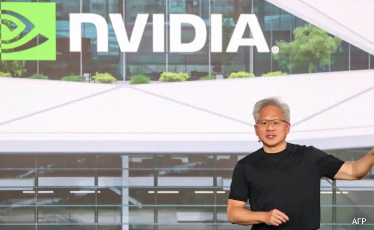
Capital expenditure in the high-performance computing sector is shifting from opportunistic procurement to infrastructure integration. Nvidia scaling its annual procurement and operational spend in Taiwan toward a target of $150 billion highlights a structural reality: compute supremacy cannot be decoupled from geographic centralization. By formalizing Project Constellation—a $1.27 billion, 50-year lease footprint at Taipei’s Beitou-Shilin Technology Park—the organization is transitioning from an fabless customer into a co-located infrastructure node.
Analyzing this move requires looking past generic narratives about regional tech hubs. The true dynamics lie in hardware co-design, extreme advanced packaging bottlenecks, and the structural dependency known as the semiconductor capital multiplier. If you liked this article, you might want to check out: this related article.
The Co-Location Flywheel: Minimizing the Distance to Silicon
The architectural complexity of modern accelerator hardware, such as the Blackwell architecture, breaks down the traditional boundary between semiconductor design and physical manufacturing. Hardware design is no longer a linear sequence where a file is sent to a contract foundry for processing. It is an iterative, highly interactive feedback loop.
Locating an advanced engineering headquarters with 4,000 personnel in close proximity to Taiwan Semiconductor Manufacturing Company (TSMC) addresses a major friction point in hardware development: late-stage engineering optimization. For another angle on this event, see the recent update from Reuters Business.
+---------------------------------------------------------+
|                  NVIDIA CONSTELLATION                   |
|               (System Architecture & Design)            |
+---------------------------------------------------------+
                            │ ▲
      Iterative Hardware    │ │  Co-Design Feedback Loop
      Optimization Paths    ▼ │
+---------------------------------------------------------+
|             TSMC ADVANCED PACKAGING ECOSYSTEM           |
|            (CoWoS-S / High-Density Substrates)          |
+---------------------------------------------------------+
This optimization bottleneck occurs primarily at the interface of advanced silicon packaging. As accelerators shift from single-die monolithic silicon to multi-chip modules, the physical interconnect length between compute units becomes the primary determinant of performance. Designing at this scale requires managing sub-micron alignment, thermal dissipation coefficients, and complex power-delivery networks.
By basing high-level systems architecture and design verification teams directly within the Taipei tech corridor, the organization achieves several structural advantages:
- Silicon Run-Time Compression: The physical proximity of design verification engineers to fabrication facilities cuts down on the time required to analyze material anomalies, layout errors, and yield deviations.
- Interconnect Optimization: Designing high-bandwidth interfaces requires direct access to the manufacturing floor to adjust for minute shifts in material characteristics, which directly impact signal loss.
- Thermal-Mechanical Co-Engineering: Managing thermal performance across multi-chip modules requires specialized testing infrastructure that can simulate high-wattage workloads alongside the foundry’s packaging engineers.
Advanced Packaging as a Supply-Chain Bottleneck
The scaling of artificial intelligence hardware is constrained less by lithography limits than by advanced backend packaging capabilities, specifically Chip-on-Wafer-on-Substrate (CoWoS) workflows. Silicon substrate fabrication acts as a strict volume ceiling for advanced AI chips.
   [ Silicon Ingot Production ]
                │
                ▼
     [ Monolithic Wafer Fab ]
                │
                ▼
  +───────────────────────────+
  │   ADVANCED PACKAGING      │ <--- System Production Volume Ceiling
  │   - CoWoS Interposers     │      (Target of Capital Integration)
  │   - HBM3e Stack-up        │
  +───────────────────────────+
                │
                ▼
  [ System Assembly / Testing ]
The physical assembly of an accelerator requires placing high-bandwidth memory (HBM3e) stack-ups adjacent to logic dies on a passive silicon interposer. This process demands tolerances that cannot be managed over long distances or distributed across disconnected supply chains.
The concentration of advanced packaging capital in Taiwan creates an economic gravity well. Competitors attempting to scale alternative compute fabrics face a stark choice: build a separate supply network from scratch or locate their operations in the same tight geographic cluster. Advanced Micro Devices (AMD) committing over $10 billion to expand its presence across the Taiwanese packaging ecosystem highlights this dynamic.
Capital allocation in this context is driven by structural necessity. Upstream silicon manufacturing, midstream packaging, and downstream board assembly via networks like Foxconn, Quanta, and Wistron are deeply interconnected. An organization cannot scale its output to meet soaring hardware demands without inserting its engineering teams directly into this continuous manufacturing pipeline.
The Geopolitical Risk Profile and Capital Concentration Risk
A highly concentrated asset footprint brings clear vulnerabilities. Concentrating massive corporate investments, core design teams, and production capacity within a single geographic region creates a single point of failure.
| Risk Core Variable | Operational Consequence | Mitigation Feasibility |
|---|---|---|
| Geopolitical Disruption | Disruption of global silicon supply, halting high-performance infrastructure deployment. | Low; replication of sub-2nm foundry capacity takes years. |
| Resource Deprivation | Grid instability or water shortages interrupting continuous fabrication runs. | Moderate; requires direct enterprise capital investment in local infrastructure. |
| Clustered Engineering Defection | Talent poaching and intellectual property compression among concentrated competitors. | Low; local human capital constraints create zero-sum hiring dynamics. |
The most immediate risk is the vulnerability of the regional energy infrastructure. Advanced chip manufacturing and high-throughput system validation are highly power-intensive processes. Sub-3nm fabrication facilities require continuous, high-megawatt power delivery; even minor voltage drops can ruin entire production runs.
The decision to scale regional investment depends on the local energy grid's ability to maintain high resilience while supporting rapid industrial growth.
Furthermore, concentrating advanced design facilities within the same technical corridors creates a highly competitive talent landscape. With Nvidia, AMD, and major regional tech firms all expanding their footprints in Taipei, the market for specialized system engineering talent becomes a zero-sum game. This localized competition drives up operational costs and accelerates talent turnover, which can introduce friction during critical chip development cycles.
Orchestrating the Hardware Stack
The allocation of $150 billion in annual spending signals a broader strategic pivot: the transformation of a hardware component vendor into an integrated system factory coordinator.
Modern high-performance computing architecture is no longer defined by the individual graphics processing unit (GPU). Instead, the system itself is the modern compute unit. Scaled infrastructure deployment requires managing the entire computing stack, from the foundational silicon to the networking fabrics and software layers.
+-------------------------------------------------------+
|                 SYSTEM COMPUTING STACK                |
+-------------------------------------------------------+
|  SOFTWARE LAYER   | CUDA Platform / Enterprise Frameworks|
+-------------------+-----------------------------------|
|  NETWORK FABRIC   | InfiniBand / Spectrum-X Ethernet   |
+-------------------+-----------------------------------|
|  SYSTEM RECEPTACLE| HGX/DGX System Architecture        |
+-------------------+-----------------------------------|
|  SILICON CORES    | Blackwell Logic / HBM3e Memories  |
+-------------------------------------------------------+
An enterprise cannot build multi-chassis system architectures without deeply integrated partnerships across every layer of production. Designing complex architectures like the GB300 NVL72 liquid-cooled racks requires managing intricate hardware dependencies:
- Foundry-Level Precision: Fabricating high-density logic elements and high-bandwidth memory on advanced processing nodes.
- System-Level Engineering: Integrating liquid-cooling manifolds, high-speed NVLink connectors, and power delivery units capable of supporting multi-kilowatt server racks.
- Network Integration: Ensuring compatibility with high-speed communication standards like InfiniBand and specialized enterprise Ethernet platforms.
By positioning its primary operational and design teams directly within the manufacturing ecosystem, the enterprise reduces friction across these development phases. This structural approach allows the company to transition from delivering individual chips to delivering fully optimized, large-scale data center systems.
This strategic footprint fundamentally alters the competitive dynamics of the industry. Competitors focused primarily on design face systemic friction when trying to scale production across fragmented networks. True differentiation in the high-performance computing market is no longer achieved solely through architectural design. It requires mastering localized supply chain orchestration and securing predictable access to advanced manufacturing capacity.